Technical specification
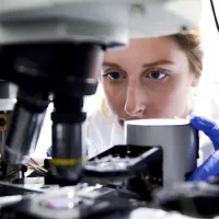
SPM systems
网络彩票APP下载_澳客彩票网-官方游戏, SPMs can be used for surface metrology analysis and electro-optical characterisation. They include:
- MultiMode V which is a high resolution system quipped with two scanners that allow scanning area of 10 ?m x 10 ?m x 2.5 ?m(XYZ) and 125 ?m x 125 ?m x 5 ?m (XYZ)
- integrated SPM and Raman system which is a combination of the Nanonics MultiView 4000 and the Renishaw inVia laser Raman spectrometer
- Nanonics CryoView 2000 which is designed to operate at temperature less than 10 K and vacuum pressure of 5 X 10⁻⁸ Torr.
- Caliber which is a versatile and high performance SPM system designed for multifunctional and routine microscopy
Zeiss EVO LS25 life science SEM
网络彩票APP下载_澳客彩票网-官方游戏, environmental SEM is specially designed to allow imaging in liquids. This means biological samples can be imaged without the problems that arise from sample dehydration. The system also has integrated X-ray functionality and forms part of the 3D X-ray imaging facility. The system provides:
- resolution of 3nm at 30kV
- 10nm at 3kV and 20nm at 1kV
- XRADIA nanoXFi fluorescence imaging spectrometer for high resolution elemental analysis
- IFG iMOXS X-ray source for trace elemental analysis
- Gatan XuM for X-ray computed tomography
Jeol JSM 7500F FESEM
网络彩票APP下载_澳客彩票网-官方游戏, FESEM provides higher resolution imaging than the environmental SEM. Its main use is for specimen imaging after electron beam lithography. It:
- resolution of 1nm at 15kV,
- operates between 0.5 and 30kV
- magnification which can be varied from '100 to '1,000,000.
Zeiss NVision 40 FIB system
The FIB system is a multi nanofabrication tool system capable of performing sophisticated nanomachining, in-situ metal or insulator deposition, lithography and metrology analysis. It provides:
- three dimensional ion beam milling
- electron microscopy dual beam technology
- metallic and insulator deposition feature
- gas injection system (GIS) unit providing deposition material such as tungsten, carbon and silica.
- xenon difluoride for in-situ nano-etching
- water for vapour assisted sample imaging
Zeiss Orion helium ion microscope
This microscope uses helium ions for surface imaging and analysis. It is ideal for nanostructure characterisation. It offers:
- resolution of less than 0.9nm at an energy of 25-30kV
- beam currents between 1fA and 25pA
- analysis of material composition using Rutherford backscattering.
Thermo Scientific? Theta Probe
网络彩票APP下载_澳客彩票网-官方游戏, high performance XPS system is designed for ultra-thin film analysis. XPS analysis can reveal information about the electronic structure of the material surface. The probe offers:
- microfocused X-ray source to measure the chemical state of the surface of complex thin films
- a dual-beam charge compensation for insulator analysis.
Woolham M-2000 spectroscopic ellipsometer
The ellipsometer is used to measure film thickness and refractive index after material deposition. It provides:
- high speed and a wide wavelength range, with automated angle (40-90 degrees) and integrated focussing
- spot size of 150 micron
- spectral range of 190-1000nm
- a liquid cell to allow thickness measurements in liquids
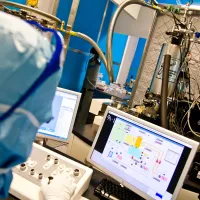
Probe stations
We also host a range of electrical characterisation systems for both commercial and research purposes. These include:
- Lakeshore EMTTP4 Cryogenic Probe Station which will allow magneto-resistance measurements from 10K and 300K without the necessity of bonding the contacts.
- Cryogenic Ltd Cryogen free cryomagnet system which is suitable for single and few electron device measurements and other fundamental research on nanoscale devices
- Sula DLTS with Janis Optical Cryostat for deep level transient spectroscopy which will allow unique electronic characterisation of materials.
- MSA-400 Micro System Analyse which provides measurements of structural vibrations and surface topology in microstructures such as MEMS
- 8 inch Cascade SUMMIT 12000B Semi-Automatic probe station with Agilent N5250A 67GHz Vector Network Analyzer which allows S-parameter measurements and other RF measurements to a high precision
- Cascade R32 REL3200 Probe-Station for any top-contact electron device
- Cascade M150 Probe Station for resistivity measurements on wafers up to 8 inch
CAD tools and modelling programs
网络彩票APP下载_澳客彩票网-官方游戏, CAD tools can be used to simulate a wide range of devices, systems and processes:
- semiconductor devices
- photonic devices
- MEMS/NEMS
- microfluidic systems
- fabrication processes
- systems and circuits