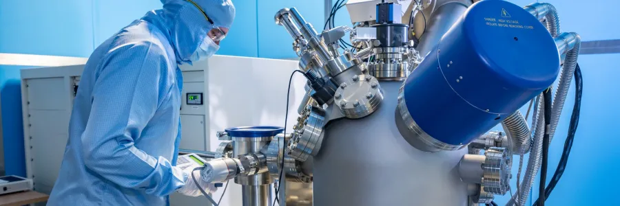
Part of the nanofabrication cleanrooms
Scanning electron microscope (SEM) systems
- JEOL IT-800i for ultra high-resolution imaging at the nanoscale across a 200mm wafer.
- Zeiss NVision 40 for high-resolution and cross-sectional imaging of devices for wafers up to 100mm in diameter. Cross-sectional imaging is focused ion beam (FIB) assisted.
- Hitachi Critical Dimension (CD) SEM. This automates high-throughput measurements of 200mm wafer photoresist profiles. The CD-SEM supports deep-ultraviolet (DUV) scanner processing.
We also have a Zeiss EVO SEM for lower-resolution work and energy-dispersive X-ray Spectroscopy (EDS). This tool is mainly used to support photonic devices research and sits outside the cleanrooms. It features a variable pressure capability for imaging and elemental analysis of a wide variety of materials.

Measurement tools
We measure thin film thickness and optical properties using ellipsometry. Stylus and optical profilometry is used to determine feature topography, wafer deflection and 3 dimensional stress. Ultra-high vacuum (UHV) X-ray photoelectron spectroscopy (XPS) enables elemental investigation at the surface of up to 50mm samples. An in-situ argon sputter gun enables cyclical depth profile measurements of elemental presence.
We characterise optical properties of materials using Raman and laser spectroscopy. We also have a wide range of?electrical and radio frequency (RF) testing equipment. These are?mounted on probe stations across our measurement laboratories.

Processes and equipment
Characterisation
- Jeol IT-800i SEM for 200mm wafer ultra high-resolution measurement of sensitive resists
- Zeiss NVision40 SEM/FIB for cross-sectional imaging down to the nanoscale
- Zeiss EVO LS25 SEM for variable pressure analysis and EDS
- Hitachi CD SEM, 200mm cassette loading
- XPS for surface analysis of elemental presence, up to 50mm substrates
- spectroscopic ellipsometry, 200-2500 nanometres, 120 micrometres spot size, up to 300mm wafer
- stylus profilers up to 200mm wafer
- Zemetrics ZeScope Optical Profiler up to 200mm wafer
- Atomic force microscopy
- 200mm wafer capable optical microscopes, 5-150x, automated stage, 24 megapixel imaging, image stitching, and programmable image acquisition
Electrical Testing
- broad range of probe stations and analysers available for electrical testing
- dedicated micro system analyser (Polytec) with white light interferometer for static and dynamic mechanical analysis

High speed photonic device testing capabilities
Chip level testing at 1550 nanometre (nm) and 1310nm wavelengths.
Processes and equipment
Optical Modulator (TX) testing
- bit pattern generator with
- 4x differential electrical data signal sources up to 64 gigabit per second (Gb/s) on/off keying (OOK)
- or 2x differential electrical data signal sources up to 128 Gb/s OOK
- or 1x differential electrical data signal sources up to 128Gb/s pulse amplitude modulation-4 (PAM-4)
- digital communications analyser (DCA) with optical input bandwidth up to 70 gigahertz (GHz)
- lightwave component analyser (LCA) for electro-optic (EO) bandwidth measurements up to 110GHz
Photodetector testing
- optical data signal can be produced with commercial LiNbO3 modulator and above BPG, however the commercial modulator is limited to 40GHz
- digital communications analyser (DCA) with electrical input bandwidth up to 80GHz
- lightwave component analyser (LCA) for EO bandwidth measurements up to 110GHz

Contact us
For more information or to book the facilities, get in touch: zepler.cleanrooms@soton.ac.uk
