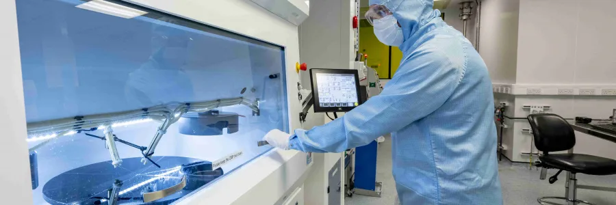
Part of the nanofabrication cleanrooms
CMP is an important capability, with multiple applications during semiconductor device fabrication. It is a part of:
- planarisation during the complementary metal-oxide-semiconductor (CMOS) process
- backend integrated circuit (IC) manufacturing including re-distribution layers (RDL)
- wafer via and through silicon via (TSV) creation
- thin film thinning
- post-trench fill planarisation
- micro-electromechanical systems (MEMS) and opto-MEMS fabrication
We have 3 Logitech CM62 tools. These provide dedicated routes for non-metal, metal, and copper processing.
We use dynamic customised polishing templates. This allows processing of almost any size or shape sample, up to 200 millimetre (mm) wafers.
These tools are ideal for scale up of research processes to pilot line production level equipment.
Processes and equipment
Logitech ORBIS CM62
- 200mm, 150mm, and 100mm static templates for SEMI standard wafer processing
- dynamic template fabrication for diced substrates, irregular shape substrates, and non-SEMI standard wafers
- dynamic template sample overhang adjustable via backing shims
- twin peristaltic pumps control slurry capacity through two separate nozzles. Different slurries can be used in each pump if required
- adjustable slurry dilution via in-situ mixing with water
- choice of hard or soft polishing pad, with diamond or brush conditioners
- standard slurries available for silicon and silicon dioxide (SiO2) polishing, other slurries possible on request
Contact us
For more information or to book the facilities, get in touch:
