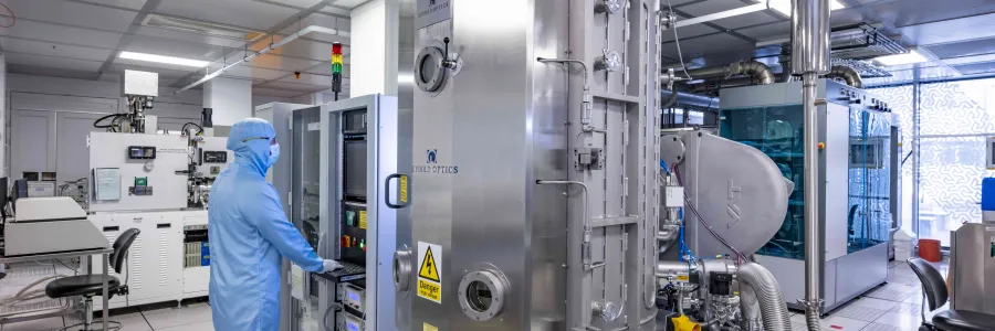
Part of the nanofabrication cleanrooms
The nanofabrication cleanrooms offer a wide range of capabilities for thin film vacuum deposition of:
- metals
- dielectrics
- semiconductors
- chalcogenides
- organic materials
Deposited thin film thicknesses typically range from nanometres (nm) to several micrometres (ІЬm). We can accommodate up to 200 millimetre (mm) wafers, non-SEMI standard wafers, diced substrates, and flexible substrates.
There may be limitations on compatible materials and substrates, depending on the tool and process required.

Processes and equipment
Evaporation
- short throw resistance and electron beam evaporation for up to 100mm wafers. Metal, dielectric, organic and chalcogenide capable
- long throw electron beam evaporation for lift off, single wafer or up to 4 simultaneous 200mm wafer processing. Ion beam assisted deposition and wafer pre-cleaning, constantly variable angle stage (single wafer load only). Metal and dielectric capable
Sputtering
- Radio Frequency (RF), pulsed Direct Current (DC), and DC sputtering of metals up to 200mm wafer
- RF and pulsed DC reactive sputtering of dielectrics up to 200mm wafer
- RF sputtering of dielectrics and chalcogenides up to 150mm wafer
- high temp sputtering to 500ЁуC, up to 200mm wafer
- production capable 12x200mm wafer mid-kilohertz sputtering tool for metals and dielectrics, high-rate oxides, low-loss optical applications, and volume work
- ion beam deposition for up to 100mm wafer
Plasma Enhanced Chemical Vapour Deposition (PECVD)
- non-metal PECVD for up to 200mm wafers at 400ЁуC, to deposit silicon dioxide (SiO2) via gas phase or TEOS, silicon nitride (Si3N4), amorphous silicon, amorphous germanium, and in-situ boron and phosphorus doping
- metals-capable 900ЁуC PECVD carbon nanotubes (CNT) growth, silicon nanowire growth, deposition of amorphous and polysilicon, amorphous germanium, silicon carbide (SiC), and boron nitride (BN). In-situ boron and phosphorus doping, and high-temperature plasma assisted annealing
Low Pressure Chemical Vapour Deposition (LPCVD)
- non-metal amorphous silicon and polycrystalline silicon deposition for up to 25x200mm wafers
- non-metal low stress or stoichiometric silicon nitride (Si3N4) deposition, for up to 25x200mm wafers
Atomic Layer Deposition (ALD)
- thermal ALD for up to 200mm wafer, exposure and boost mode for high aspect ratio feature coating, up to 300ЁуC, water and ozone reactants
- plasma-assisted ALD for up to 200mm wafer size, oxides and nitrides, up to 400ЁуC
- aluminium, zinc, hafnium, titanium, tungsten, molybdenum, nickel, vanadium dielectrics demonstrated. Other sources considered
Furnace Oxidation
- non-metal dry and wet thermal oxidation up to 1000ЁуC for 100-200mm wafers
- dry thermal oxidation up to 1000ЁуC for 100-150mm wafers with some metals permitted

Contact us
For more information or to book the facilities, get in touch: zepler.cleanrooms@soton.ac.uk
